Research:
The Center for Nanophotonics conducts research and development on manipulation of photons-electrons in nano-scale materials for innovative photonic devices and emerging technologies. The Center’s research areas cover a broad spectrum, ranging from basic to applied, and dealing with state-of-the-art nano-scale material synthesis, fundamental physics, device fabrication and testing.
In particular, our research is dedicated to the advancement of III-nitride wide bandgap semiconductors (BN, GaN, AlN, AlGaN, InGaN, and InAlGaN). These materials have contributed on the grandest scale to many technological advances including UV/blue/green/white LEDs, solid-state lighting, UV/blue/green laser diodes, UV/visible detectors, and high temperature/power transistors. Our group’s concentration areas are epitaxial growth, micro- and nano-structure and device fabrication, and fundamental optical and transport investigations. We have pioneered the developments of the following emerging technologies:
- We are the inventors of micro-LEDs Ι patent link. Emerging technologies including single-chip high voltage DC/AC-LEDs, micro-LED displays and self-emissive microdisplays were all evolved from III-nitride micro-LED and array technology first invented by our group. doi: 10.1063/1.1351521 Ι PDF; doi: 10.1063/1.1326479 Ι PDF; doi: 10.1117/2.1201112.004001 Ι PDF Ι News
- Growth of wafer scale (up to 4-inch in diameter) hexagonal boron nitride (h-BN) epitaxial layers by MOCVD. Hexagonal boron nitride materials with large size wafers will be highly useful for deep ultraviolet photonics/optoelectronics, neutron detection, graphene electronic and photonic devices; doi: 10.1063/1.3593958 Ι PDF; doi:10.1088/0268-1242/29/8/084003 Ι PDF Ι News
- Achieved h-BN thermal neutron detectors with 51.4% detection efficiency, which is a record high for semiconductor thermal neutron detectors. doi: 10.1063/1.4960522 Ι PDF Ι News
- Demonstrated the first active driving full scale high-resolution self-emissive blue/green microdisplays capable of delivering video graphics images for high brightness pico-projector and head-up/wearable display applications; doi: 10.1063/1.3615679 Ι PDF; doi: 10.1117/2.1201112.004001 Ι PDF Ι News
- Deep UV LEDs and deep UV and extreme UV detectors based on III-nitrides for applications of probing intrinsic fluorescence in protein, equipment/personnel decontamination, photocatalysis, EUV metrology and astronomy; doi: 10.1063/1.1879098 Ι PDF; doi: 10.1063/1.1914960 Ι PDF; doi: 10.1063/1.2823588 Ι PDF; doi: 10.1063/1.2397021 Ι PDF Ι News
- Demonstrated the first InGaN quantum well solar cell for improved solar conversion efficiency; doi: 10.1063/1.3081123 Ι PDF Ι News
- InGaN photoelectrochemical cells for hydrogen generation and energy storage;
- Thermoelectrics based on InGaN and InAlGaN alloys for converting waste heat to electricity; doi: 10.1063/1.2839309 Ι PDF
- Achieved the first current injection Er doped GaN 1.5 micron LEDs and integration of Er doped GaN 1.5 micron light-emitting devices with CMOS compatible Si (100) substrates for Si photonics and optical communications; doi: 10.1063/1.3499654 Ι PDF; doi: 10.1063/1.3556678 Ι PDF Ι News
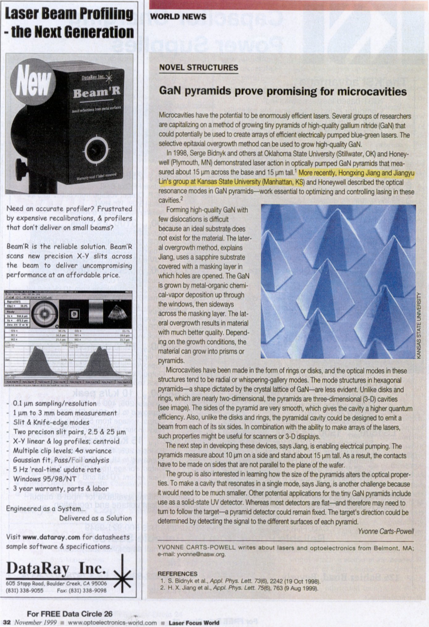
- Our work on the fundamental optical transitions in III-nitrides has revealed that, as a direct consequence of the band structure of AlN, the TM mode is the dominant laser emission in UV laser diodes (LDs) using high Al-content AlGaN as active layers, in contrast to all other semiconductor LDs in which the TE mode is the dominant lasing emission. This revelation will have a significant implication on the future design of UV LDs based upon AlGaN; doi: 10.1063/1.1765208 Ι PDF; doi: 10.1063/1.1633965 Ι PDF
- By minimizing the density of native defects, our group has achieved high Al content AlGaN alloys with record high conductivities and expanded active photonic materials into the deep UV spectral range down to 200 nm; doi: 10.1063/1.1809272 Ι PDF; doi: 10.1063/1.1879098 Ι PDF
- Our group’s contributions to the advancement of science also include the development of the very first DUV picosecond time-resolve photoluminescence spectroscopy system (from 3 mm to 195 nm) for probing fundamental properties of excitons and free carriers and their dynamics in a wide range of nano-scale materials;
- III-nitride photonic crystal LEDs with feature size in sub-100 nm range, demonstrated first by our group, are being recognized as one of the most prominent technologies to boost the LED efficiency for solid-state-lighting technology; doi: 10.1063/1.1600839 Ι PDF; doi: 10.1063/1.1644050 Ι PDF; doi: 10.1063/1.1768297 Ι PDF
- Successfully realized the first blue LED on 6-inch Si substrate; doi:10.1063/1.2199492 Ι PDF Ι News
Find out more about our research at our Research Areas page.
Our current research is supported by
DOD Joint Technology Office (JTO)/Air Force Research Laboratory/Office of Naval Research
DOE (ARPA-E)
Professor Hongxing Jiang and Professor Jingyu Lin were the team members of the following research programs:
BMDO GAMPA Program
DARPA SUVOS Program
DARPA VIGIL Program
DARPA DUVAP Program
DARPA CMUVT Program
DHS (ARI Research Program)
Our research was also supported by
DOE (BES and NNSA)
ARO
NSF
The founding of the TTU Nanophotonics Center would
not have been possible without the support of
Mr. Ed Whitacre and the AT
& T Foundation.
Contact Information:
Dr. Hongxing Jiang, Ed Whitacre Endowed Chair and Horn Professor
Tel: (806) 834-5739
Fax: 806-742-1245
hx.jiang@ttu.edu
Dr. Jingyu Lin, Linda Whitacre Endowed Chair and Horn Professor
Tel. (806) 834-5383
Fax: 806-742-1245
Jingyu.lin@ttu.edu
Dr. Jing Li, Research Professor
Tel. (806) 742-3462
Fax: 806-742-1245
Jing.li@ttu.edu
Postal address:
Nanophotonics Center
Engineering and Technology Lab Building
10th and Akron Ave.
Texas Tech University
Lubbock, TX 79409